| Make |
: JEOL
|
| Model |
: JEM 2100F
|
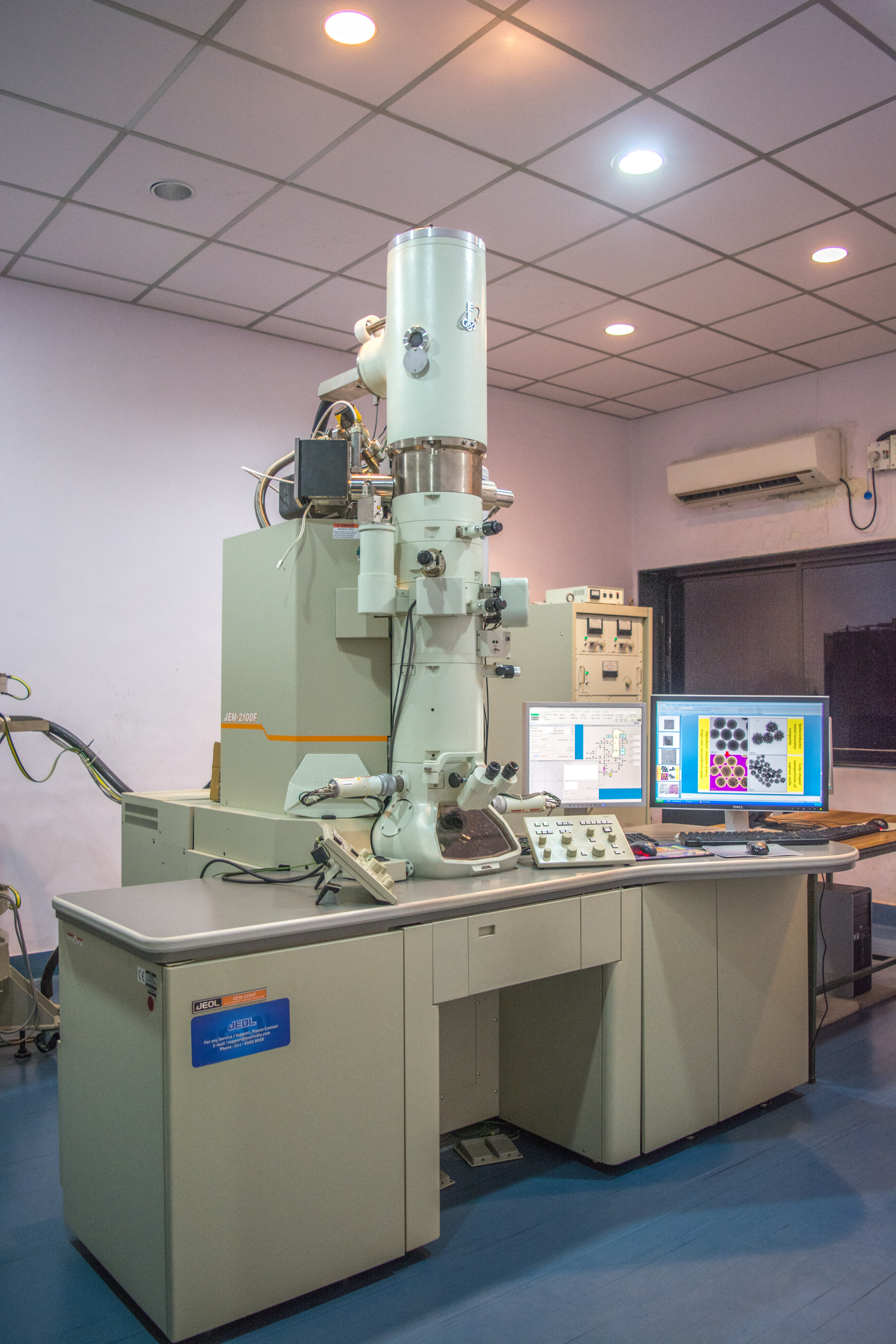 |
| Specification |
:
Resolution : Point : 0.19 nm Line : 0.1 nm
Magnification : 50 x - 1.5M x
Accelerating Potential : 120kV and 200 kV
|
|
 Nano science/Nano Technology Nano science/Nano Technology
Micro/Nano electronics
Thin Films
Catalysis
Corrosion
Polymer science
Energy science/Engg.
Biological and life sciences
|
FEG TEM 200 kV Lab, Ground Floor,
CRNTS/SAIF, IIT Bombay
|
External Users( Other than IIT Bombay):
1. A requisition letter addressed to Head, SAIF along with a printout of electronic fund transfer (NEFT) proof should be sent by post or submitted in
person to SAIF office, IIT Bombay, Powai, Mumbai-400076.
2. Once we receive the requisition letter and advance payment, your appointment will be scheduled as per the queue.
3. The user will be informed about the appointment date and time by e-mail.
4. The sample can be loaded on a carbon coated copper grid or can be made in disc form, 3mm diameter, with a thinned (electron transparency) central area.
5. It is desirable that the user is present in the FEG-TEM lab at the time of appointment for better utilization of the facility.
6. Before proceeding further, please review How to Use Facility and Payment Procedure for more information.
Internal (IIT Bombay) Users:
1. The user should register online.
2. An appointment will be given as per the queue and the user will be informed by an email.
3. The new user is requested to contact FEG-TEM Lab before registration.
|
|
|
All queries regarding sample analysis and charges should be sent only on fegtemlab@iitb.ac.in.
|
|
|
Head, CRNTS/SAIF IIT Bombay
Email Id : head.crnts@iitb.ac.in
|
Contact : 022-2159 6865
Email Id : fegtemlab@iitb.ac.in
|
|
FEG TEM 200 kV Samplewise format, Charges includes Grid and GST for External users
|
| | Industry | University | National Lab/R&D's | IIT Bombay Users | |
| Imaging
| 10325/- | 2065/- | 4720/- | 875/- | Per Sample
|
|
|