|
|
|
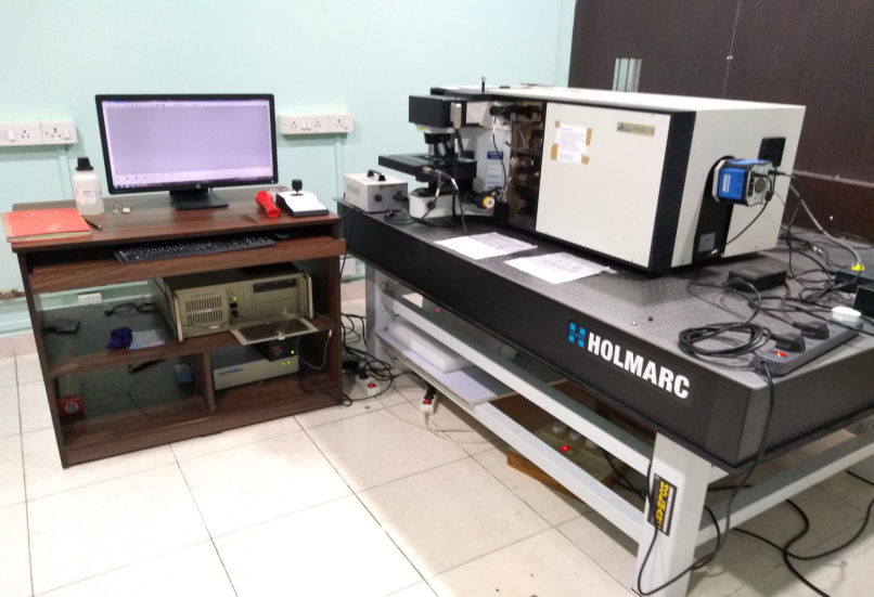
Laser Raman Spectroscopy (LRS)
|
 Kindly download Material Safety Data sheet and submit the hardcopy of filled sheet along with your sample Kindly download Material Safety Data sheet and submit the hardcopy of filled sheet along with your sample
| Make |
: Horiba Jobin Yvon, France |
| Model |
: HR800-UV confocal micro-Raman spectrometer
|
 |
| Specification |
:
Single stage grating spectrometer of 800 mm focal length with two gratings mounted back to back.
 Olympus BX41 microscope with confocal collection system. Olympus BX41 microscope with confocal collection system.
Excitation sources: (a) 532 nm 50 mW & 633 nm 20 mW
Gratings:
(a) 600 l/mm Low resolution large scan range ( ~15000 cm-1)
(b) 1800 l/mm high resolution ,scan range (~5000 cm-1)
Microscope Objective
Normal WD: 10X,20X,50X,100X (WD : 20,10.6,1.3,0.38,0.21 mm)
Long WD: 50X, 100X (WD: 10.6, 3.4 mm)
Imaging/Mapping
XYZ mapping:
XY stage :X=75 mm and Y=50 mm , 1 µm repeatability
Step-by-step mode : step size (min) 50 nm
Z stage: min step = 0.1 um
Duoscan Mode with scanning mirror.
1. Scanning/Averaging followed by Macro mapping
Polarized Raman Scattering
Range 400 – 700 nm
Low Temp : Min 80K
|
Laser Raman Spectroscopy is based on inelastic scattering of light from the sample and gives information on the electronic and vibrational states of the material. The Raman spectrum of a material provides a unique fingerprint, which is can be used as a non-destructive characterization tool with minimum of sample preparation.
|
Raman scattering is inelastic scattering of light and on excitation by incident and the scattered photon can be either of lower or higher energy depending on the initial state of the system before excitation. These correspond to stokes or anti-stokes Raman scattered light. The difference between the scattered and excited light frequency is known as Raman shift and measured in cm-1 and consists of several Raman lines depending on the material. These serve as 'fingerprint' for the sample and are used for sample characterization. In addition, the line-shape and linewidth of these Raman lines provide other information like crystallinity, order/disorder state of the material. This has resulted in application of this technique in research in physical, chemical, biological sciences. In a micro-Raman spectrometer the incident laser light is focused using a microscope objective lens and the scattered light is also collected by the same and reflected in to the spectrometer through the confocal hole which reduces the background noise and provides depth information. Since the incident laser and Raman scattered light are both polarized, this spectrometer is capable of Polarization dependent Raman spectroscopy for several applications. It also a microscopy compatible low temperature stage which can go down to 80K (min)
The Raman scattered light is always accompanied by the elastic scattered Rayleigh component which is 103 - 105 stronger than the Raman components which completely masks the weaker Raman signal. The Rayleigh background is removed using sharp cutoff Notch/Edge filters which allow the spectrum to be recorded as close as ~ 100 cm-1. The detection efficiency has been increased by order of magnitude using multichannel CCD detector of high QE.
This system has been recently upgraded to perform Raman imaging/mapping in XY plane both using step point scanning as well as scanning mirror for moderate to large area mapping. It can also depth mapping using the confocal property.
|
 Nano science/Nano Technology Nano science/Nano Technology
Micro/Nano electronics
Thin Films
Catalysis
Corrosion
Polymer science
Energy science/Engg.
Biological and life sciences
Chemical Composition and Quantification [EDS]
Elemental Mapping and Line Scan [STEM]
|
LRS Lab, 1st Floor,
CRNTS/SAIF, IIT Bombay
|
1. Provide solid samples in powder form. Minimum amount required 1-2 mg.
2. Samples may be in liquid form. Minimum amount required 1-2 ml.
3. Samples can be submitted as thin films, solid pallets, powder etc.
|
|
|
|
Head, CRNTS/SAIF IIT Bombay
Contact : 022-25767690
Email Id : head.crnts@iitb.ac.in
|
Mrs. Mayuri N Gandhi
CRNTS/SAIF IIT Bombay
Contact : 022-2159 6899
Email Id : lrs.crnts@iitb.ac.in,pallaviag@iitb.ac.in,mngandhi@iitb.ac.in
|
|
Laser Raman Spectroscopy Samplewise format, Charges includes Grid and GST for External users
|
| | Industry | Academic Institute | National Lab/R&D's | IIT Bombay Users | |
| Raman Analysis
|
3540/- | 708
/- | 1770/- | 300/- | Per Slot
(1 hr 30 min)
|
| Raman Imaging | 7080/- | 1416/- | 3540/- | 600/- | Per Slot (1 hr 30 min)
|
|
|
|